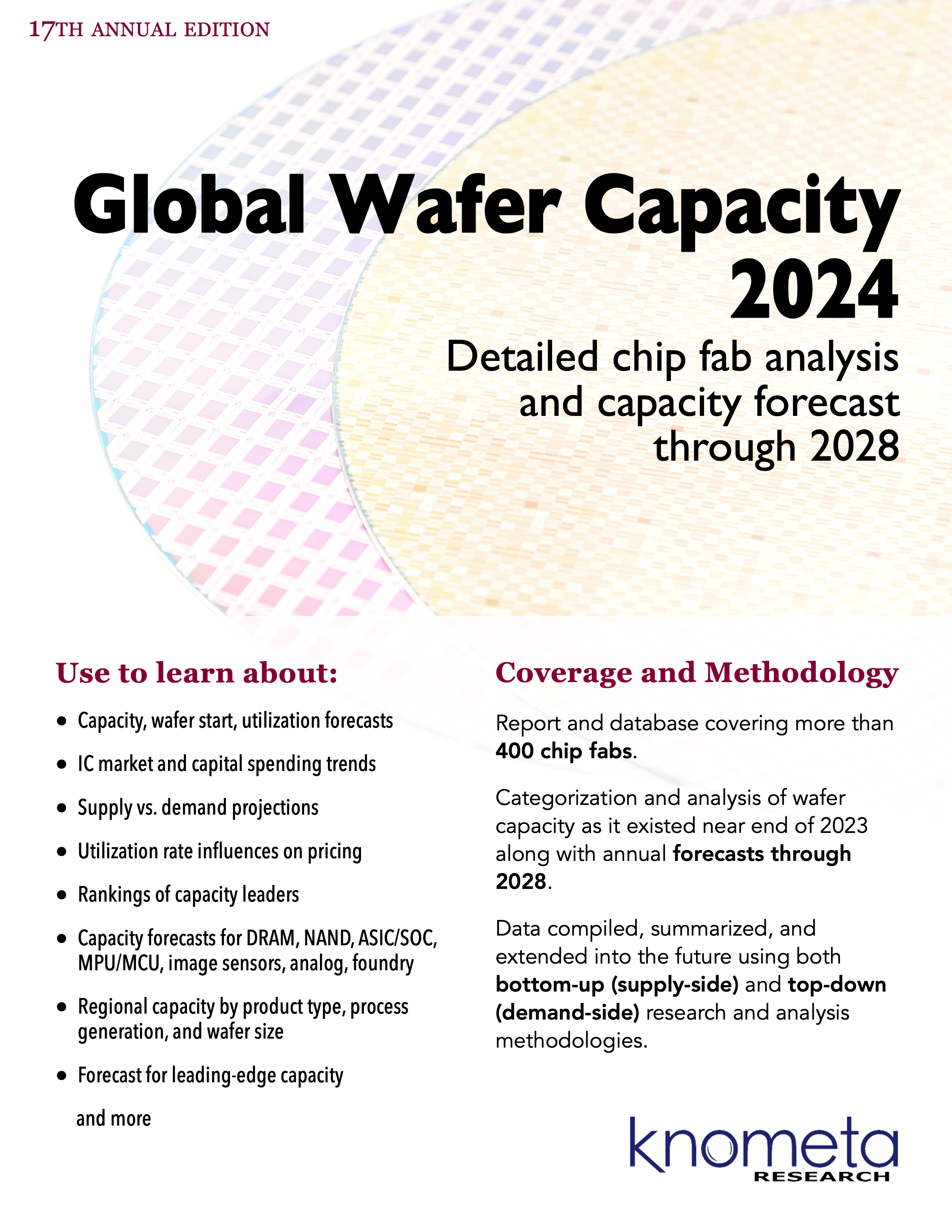
Global Wafer Capacity 2024
Detailed chip fab analysis and capacity forecast through 2028
Knometa took ownership of IC Insights' Global Wafer Capacity report in late 2021. As an IC Insights executive, Knometa's Trevor Yancey created this report in 2007 and has been the report's lead analyst and project manager every year since. Mr. Yancey has authored the report as an independent consultant since 2015.
Global Wafer Capacity report provides a detailed breakdown and analysis of the IC industry's wafer fab capacity as it stood near the end of 2023 and then forecasts capacity for each year through 2028.
Accompanying the main report are three addendums: supplemental slides that summarize trends, a spreadsheet of details for all fabs covered in the report, and a set of workbooks with spreadsheets of capacity data for charts.
The 2024 edition is the final issue of Global Wafer Capacity. There will be no further issues of the report, but the 2024 edition is still available for purchase at a significant discount.
Use to learn about:
- Capacity, wafer start & utilization forecasts
- IC market and capital spending trends
- Supply vs. demand projections
- Utilization rate influences on pricing
- Rankings of capacity leaders
- Capacity forecasts for DRAM, NAND, MPU/MCU, etc.
- Regional capacity by product type, process generation, wafer size
- Forecast for leading-edge capacity
- Detailed specifications for hundreds of semiconductor fabs
Coverage and Methodology
Report and database covering more than 400 chip fabs.
Categorization and analysis of wafer capacity as it existed near end of 2023 along with annual forecasts through 2028.
Data compiled, summarized, and extended into the future using both bottom-up (supply-side) and top-down (demand-side) research and analysis methodologies.
Data Classifications
Wafer Size
300mm, 200mm, ≤150mm
Geographic Region/Country
Americas, Europe, Japan, Korea, Taiwan, China, ROW
Product Type
Analog, DRAM, NAND, ASIC/SOC, MPU/MCU, Image Sensor, Foundry
Process Generation
Leading Edge, Lagging Edge, Mature, Large Feature
Process Type
CMOS, BiCMOS/BCD, Bipolar, III-V
Fab Details Database
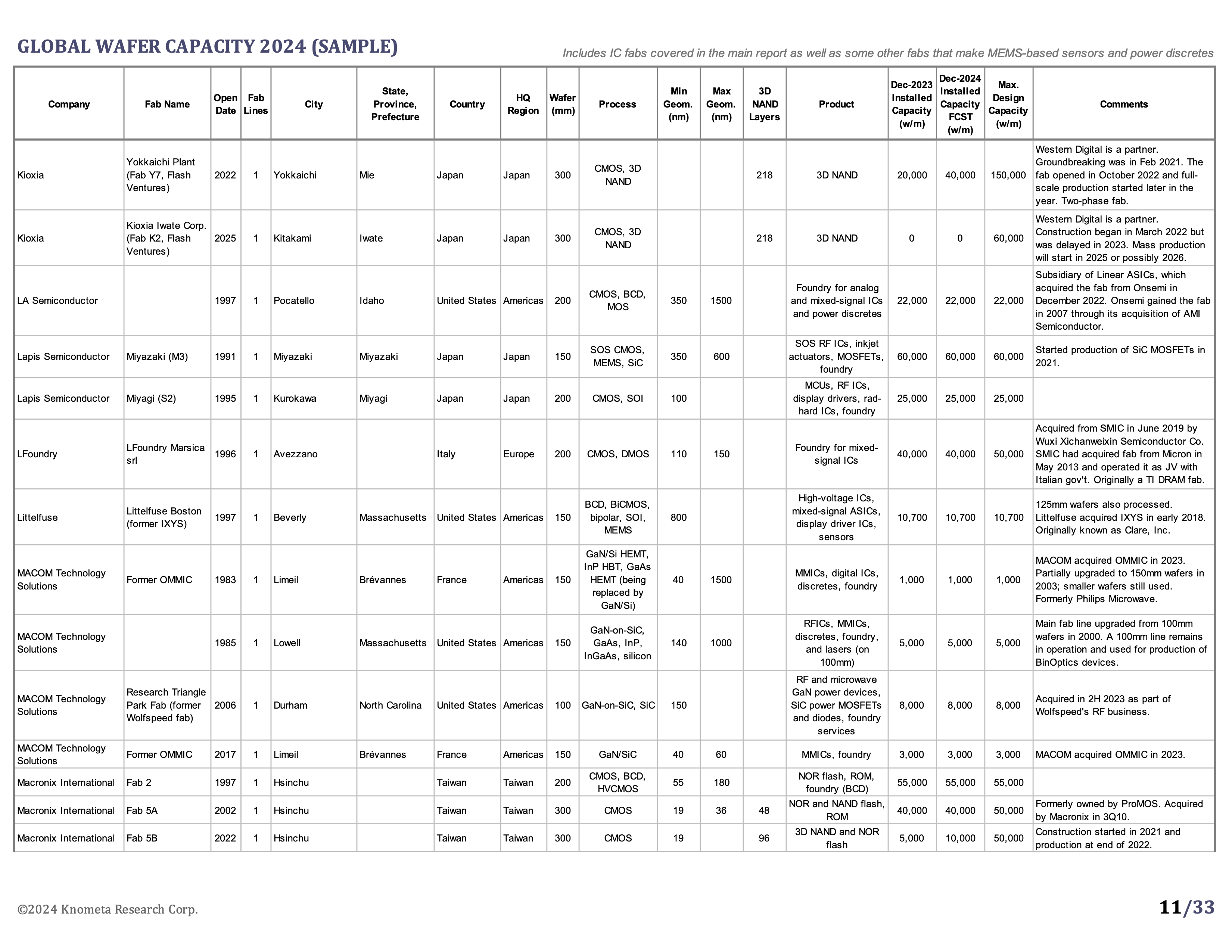
Company • Fab Name & Location • Date Opened • Wafer Size • Current & Planned Capacity • Process Technology • Products
Report Details
Published February 2024
Purchase Options
Pricing
- Single-user access:
US$5,500US$2,750 (50% off) - Multiple-user enterprise access:
US$8,400US$4,200 (50% off)
Accepted Payment Methods
- Credit/debit card
- Apple Pay
- ACH transfer
- Purchase order/wire transfer
Place Order
Once you have submitted an order, a confirmation message will be sent to you by email. If you do not receive a message, please let us know.
Orders are generally processed the same day.
Reports sold by partner TechSearch International, Inc.
Knometa Research contributes to semiconductor technology and market reports published by TechSearch International, Inc.

RECENT
- Advanced Packaging Update (APU)
- Flip Chip and WLP (Wafer-Level Packaging)
- Quantifying the Impact of Heterogeneous Integration: Chiplets & SiP
OLDER
- New Frontiers in Automotive Electronic Packaging
- SiP (System-in-Package) for Mobile Applications