Record volume of IC wafer capacity coming online in 2025
While the global economic condition remains challenging, the semiconductor market started showing signs of recovery in late 2023. Following a sharp decline in IC unit shipments in 2023, unit growth is forecast to be about 11% in both 2024 and 2025.
According to the Global Wafer Capacity 2024 report from Knometa Research, the expansion of wafer capacity in 2024 is expected to be relatively low at 4% as manufacturers let capacity utilization rates recover from the low levels experienced in 2023.
Construction started in 2022 on many fabs originally scheduled to begin operations in 2024, but the market downturn that began that year caused the start date for some fabs to be pushed out to 2025, joining many other fabs already scheduled to open during that year. The result is predicted to be a record volume of capacity brought online in 2025.
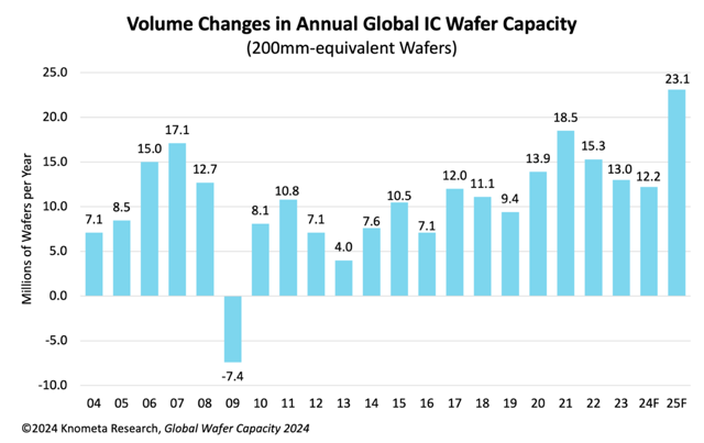
The report shows that 23.1 million 200mm-equivalent wafers per year of capacity is projected to be put into production in 2025, surpassing the previous high of 18.5 million wafers in 2021. When expressed in 300mm wafer equivalents, there will be 10.3 million wafers per year of capacity brought online in 2025. In terms of growth rate, this is an 8% increase compared to the 2024 capacity level.
According to the Global Wafer Capacity 2024 report from Knometa Research, the expansion of wafer capacity in 2024 is expected to be relatively low at 4% as manufacturers let capacity utilization rates recover from the low levels experienced in 2023.
Construction started in 2022 on many fabs originally scheduled to begin operations in 2024, but the market downturn that began that year caused the start date for some fabs to be pushed out to 2025, joining many other fabs already scheduled to open during that year. The result is predicted to be a record volume of capacity brought online in 2025.
The report shows that 23.1 million 200mm-equivalent wafers per year of capacity is projected to be put into production in 2025, surpassing the previous high of 18.5 million wafers in 2021. When expressed in 300mm wafer equivalents, there will be 10.3 million wafers per year of capacity brought online in 2025. In terms of growth rate, this is an 8% increase compared to the 2024 capacity level.
Seventeen new fab lines for IC production are scheduled to begin operations in 2025. These include the following:
The report is available for purchase here.
- HH Grace – Wuxi, China – 300mm wafers for foundry services
- Intel – New Albany, Ohio, USA – 300mm wafers for adv. logic and foundry
- JS Foundry – Ojiya, Niigata, Japan – 200mm wafers for ICs (and discretes)
- Kioxia – Kitakami, Iwate, Japan – 300mm wafers for 3D NAND
- Micron – Boise, Idaho, USA – 300mm wafers for DRAM
- Pengxin Micro – Shenzhen, China – 300mm wafers for foundry
- Samsung – Pyeongtaek, S. Korea (P4 fab) – 300mm wafers for 3D NAND and DRAM
- SK Hynix – Dalian, China (Fab 68 expansion) – 300mm wafers for 3D NAND
- SMIC – Shanghai, China (SN2 fab) – 300mm wafers for foundry
- TI – Sherman, Texas, USA – 300mm wafers for analog and mixed-signal
- TSMC – Tainan, Taiwan (Fab 18, Phase 8) – 300mm wafers for foundry
- UMC – Singapore (Fab 12i, Phase 3) – 300mm wafers for foundry
The report is available for purchase here.