Strong Growth in Wafer Capacity for Image Sensors Expected
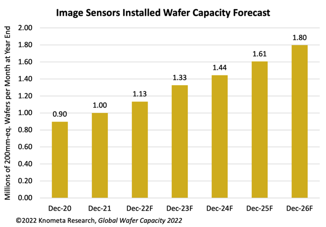
Global installed capacity for image sensors was one million 200mm-equivalent wafers per month at the end of 2021. According to the new Global Wafer Capacity 2022 report, image sensor capacity is forecast to increase 13% in 2022.
By the end of 2026, installed capacity for image sensors is projected to be 1.8 million 200mm-equiv. wafers per month. That’s an average annual growth rate of 12.5% over the forecast period, making image sensor capacity among the fastest growing segments.
While the Covid-19 pandemic negatively impacted the image sensor market in 2020, growth returned in 2021. Demand for digital imaging is increasing in virtually all areas, including cellphones, automotive, machine vision, security cameras, webcams, drones, and more.
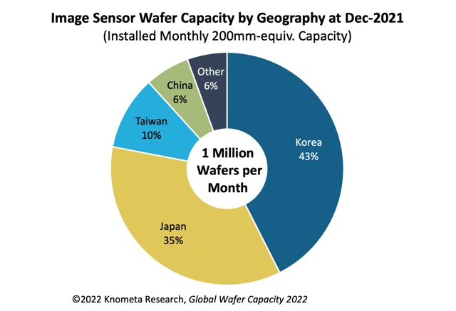
While Sony in Japan is the industry’s leading CMOS image sensor supplier, the combined CIS capacity of Samsung and SK Hynix made Korea the industry’s biggest source for production of image sensors at the end of 2021.
More than a decade ago, Sony set a goal to become the largest supplier of image sensors for cellphones. After claiming the top spot, Sony in 2014 took aim at becoming the largest supplier of CMOS image sensors for automotive systems and it is pursuing machine vision applications in factory automation and drones as well as image-recognition security cameras. Sony also sells 3D imaging sensors for depth ranging, face recognition, artificial intelligence, and machine vision.
Sony was the first to manufacture image sensors on 300mm wafers. The company has continued expanding its CIS capacity by converting 300mm fabs from logic to image sensor production and by acquiring 300mm fabs from other companies in Japan looking to exit the business of fabricating ICs. Sony has eight 300mm fab lines at four sites in Japan, with the newest being Fab 5 in Nagasaki. Fab 5 started mass production in 2021 and the construction of an expansion is already underway.
Samsung entered the CMOS image sensor business to diversify its business beyond DRAM and NAND flash. Since the fabrication technologies and tool sets for CIS devices are like that of DRAM, Samsung repurposed older DRAM fabs to begin making image sensors. The company became the industry’s second largest supplier of image sensors by serving most of the camera module needs of its huge cellphone business. Samsung’s image sensor production exists primarily at a large 300mm fab facility in Hawseong, South Korea.
SK Hynix has used the same strategy of turning older DRAM fabs into capacity for CMOS image sensors but lacks the benefit of having another related SK Hynix operation to buy its CIS devices. The company has a small but growing share of the global image sensor market.
The industry’s third largest supplier of image sensors is OmniVision but it relies on external foundries for the fabrication of its CIS wafers. OmniVision’s primary sources of foundry capacity are TSMC in Taiwan and SMIC and HLMC in China.
The Global Wafer Capacity 2022 report is available for purchase here.